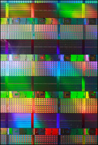
The chip is the size of a fingernail. 11 years ago...
|
A chip with 80 processing cores and capable of more than a trillion
calculations per second (teraflop) has been unveiled by Intel.
The Teraflop chip is not a commercial release but could point the way to more powerful processors, said the firm.
The chip achieves performance on a piece of silicon no
bigger than a fingernail that 11 years ago required a machine with
10,000 chips inside it.
The challenge is to find a way to program the many cores simultaneously.
Current desktop machines have up to four separate cores,
while the Cell processor inside the PlayStation 3 has eight (seven of
them useable). Each core is effectively a programmable chip in its own
right.
But to take advantage of the extra processing power,
programmers need to gives instructions to each core that work in
parallel with one another.
There are already specialist chips with multiple cores -
such as those used in router hardware and graphics cards - but Dr Mark
Bull, at the Edinburgh Parallel Computing Centre, said multi-core chips
were forcing a sea-change in the programming of desktop applications.
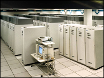
...the same computing power required 2,000 square feet
|
"It's not too difficult to find two or four independent
things you can do concurrently, finding 80 or more things is more
difficult, especially for desktop applications.
"It is going to require quite a revolution in software programming.
"Massive parallelism has been the preserve of the minority - a few people doing high-performance scientific computing.
"But that sort of thing is going to have to find its way into the mainstream."
The first time teraflop performance was achieved was 11
years on the ASCI Red Supercomputer built by Intel for the Sandia
National Laboratory.
 |
 It is going to require quite a revolution in software programming

|
That machine took up more than 2,000 square feet, was
powered by almost 10,000 Pentium Pro processors, and consumed more than
500 kilowatts of electricity.
"Our researchers have achieved a wonderful and key
milestone in terms of being able to drive multi-core and parallel
computing performance forward," said Justin Rattner, Intel Senior
Fellow and chief technology officer.
"It points the way to the near future when
teraflops-capable designs will be commonplace and reshape what we can
all expect from our computers and the internet at home and in the
office."
The Teraflop chip uses less electricity than many
current high-end processors, making the design attractive for use in
home computers.
It consumes 62 watts, and the cores can power on and off independently, making it more energy efficient.
Intel says that commercial spin-offs of the chip could
see it being used in high-definition entertainment PCs, servers and
handheld devices.
Possible uses include artificial intelligence, instant
video communications, photo-realistic games and real-time speech
recognition, said the firm.
|


 News services
 Lynne Truss
 In pictures
 Amputee cup